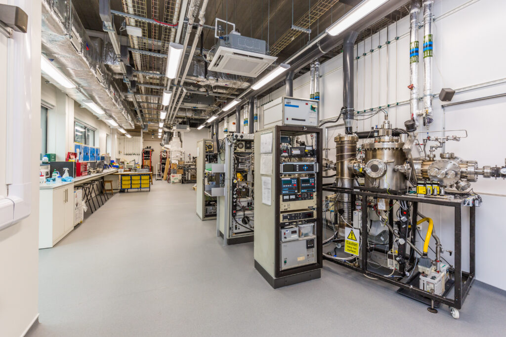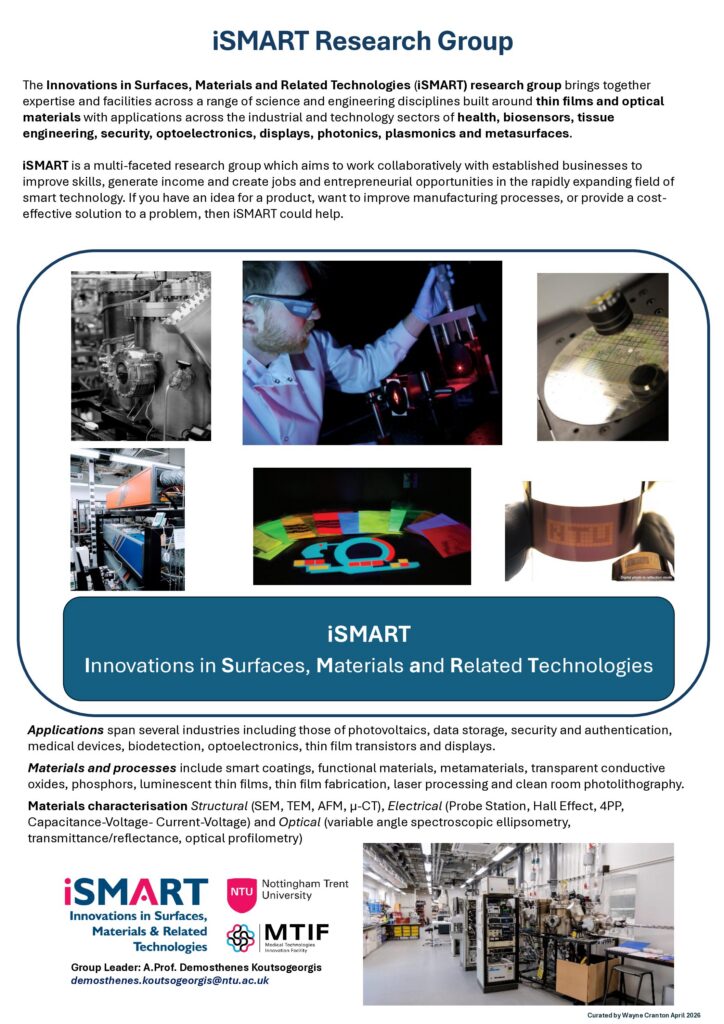
Innovations in Surfaces, Materials and Related Technologies (iSMART)
Led by Dr Demosthenes Koutsogeorgis, this pioneering research group bringing together expertise and facilities across a range of science and engineering disciplines built around thin films and optical materials. Previous work includes projects across the sectors of health, biosensors, tissue engineering, security, optoelectronics, semiconductors displays, photonics, plasmonics and metasurfaces.